New process for producing near-atomic scale silicon structures – nanobumps – developed by Cornell researchers
By David Brand
An engineer and a chemist, working together on a corporately funded research project at Cornell University, are reporting a fundamentally new way to fabricate nanoscale structures on silicon that promises the development of devices ranging from biological sensors to light-emitting silicon displays.
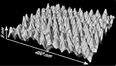
The new process, called controlled etching of dislocations (CED), has produced an array of features on a silicon surface with tiny columns – the researchers call them "nanobumps" – just 25 nanometers across (about 75 atoms) six times smaller than the width of the most minuscule component of a commercial microprocessor. (A nanometer is equal to the width of 3 silicon atoms.)
The microelectronics industry uses optical lithography, essentially photographic reduction, to produce microscopic devices, such as computer circuitry. But the technique is limited by the wavelength of light, and to date, commercial optical lithography has not been able to produce features smaller than 150 nanometers in width.
The Cornell researchers, Stephen Sass, professor of materials science and engineering, and Melissa Hines, associate professor of chemistry and chemical biology, believe that the new etching process will enable them to produce silicon structures as small as 10 nanometers, which is the distance between binding sites on a human antibody. "We now have the tools to make very fine-scale surface features at the length scale of biologically important molecules, such as human antibodies" says Sass. "We would hope to develop properties and applications we can't even imagine today."
Sass and Hines note that a process based on CED can potentially produce tiny structures across an entire six-inch silicon wafer, suggesting that the technique can easily be scaled up for industrial production. "I like to think of this as creating nano-Lego surface structures, which ultimately we can build on to make a variety of devices," says Sass. The researchers report their findings in a forthcoming issue (April 9) of Applied Physics Letters , a publication of the American Institute of Physics.
"This work provides an interesting new approach to creating arrays of periodic nanostructures on a semiconductor surface," comments Harold Craighead, director of the Cornell Nanobiotechnology Center, where part of the research was performed. "If one can create large areas of precisely controlled objects, some of the problems associated with random sizes on depositions could be reduced."
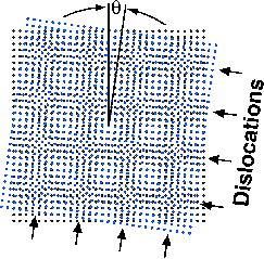
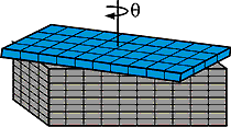
Sass notes that the theory behind CED has been known for a long time. In their process, two identical silicon wafers are twisted, one against the other, at a precisely controlled angle, and then are bonded together to make a bicrystal. Because of this twist angle, rows of atoms in the two wafers don't line up correctly. Only where the rows cross each other do the atoms line up and form strong bonds. The result is a repeating atomic scale mismatch that can be simulated by a moiré pattern.
Moiré patterns are common in everyday life and often occur when two repeating patterns overlap one another. They can be seen in folds of sheer curtains and in reflections of window screens. The atomic-scale moiré pattern created at the interface of the silicon wafers looks like a checkerboard. A QuickTime demonstration of the pattern can be seen online at http://www.chem.cornell.edu/mah11/Nanofab.html .
Sass has studied the interfaces between crystals – called grain boundaries – for 30 years. In some regions (the squares of the moiré "checkerboard"), the atoms line up correctly and, therefore, are strongly bonded. In other regions (the lines around the squares of the checkerboard), the atoms are poorly bonded. The twist angle controls the size of the checkerboard, so that large angles give small spacings, while small angles give large spacings.
Using a solution of chromium trioxide and hydrofluoric acid, the Cornell researchers etched away the lines of poorly bonded atoms, which are called dislocations, and produced an array of nanobumps. To prove their concept, the researchers fabricated a test structure with nanobumps that were approximately 100 atoms (25 nanometers) in diameter and 160 atoms (38 nanometers) apart. (See image.)
Sass and Hines calculate that if a silicon bicrystal were fabricated with a twist angle of 4 degrees, in principle, nanobumps just 5.5 nanometers in width, or about 20 atoms, could be created.
In fact, it is not the width of the nanobumps that matters so much as the distance between them. Because this spacing decreases as the twist angle of one silicon crystal relative to the other increases, says Sass, an angle of 10 degrees would produce a distance between nanobumps of only two nanometers (about 6 silicon atoms), "although we really don't know what the limit of this technique is." Nanofabrication at these near-atomic length scales has many potential applications, says Hines. The new technique potentially opens the door to manufacturing at biological dimensions because many molecules, such as human antibodies, have features on a similar scale. Other technology possible with CED, says Hines, might be light-emitting silicon devices. Normally silicon does not emit light. But in microscopic fragments of silicon, electrons are confined and travel in a way that allows them to emit light. "That might mean that you could make a flat-panel display for a computer out of the same stuff you use to make the computer itself," she says.
In addition, magnetic material could be deposited on the nanobumps to create a high-density data storage medium. "Experience has taught us one thing, though. Every time we have learned to machine at a smaller length scale, new applications have emerged. And they have never been the actual applications we originally dreamed of," Hines says.
The research was funded by a $2.8 million, three-year grant from Philip Morris Inc.
Media Contact
Get Cornell news delivered right to your inbox.
Subscribe