Smallest guitar, about the size of a human blood cell, illustrates new technology for nano-sized electromechanical devices
By Larry Bernard
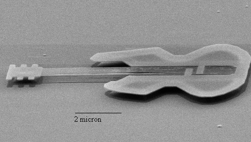
The world's smallest guitar — carved out of crystalline silicon and no larger than a single cell — has been made at Cornell University to demonstrate a new technology that could have a variety of uses in fiber optics, displays, sensors and electronics.
The "nanoguitar" — made for fun to illustrate the technology — is just one of several structures that Cornell researchers believe are the world's smallest silicon mechanical devices. Researchers made these devices at the Cornell Nanofabrication Facility, bringing microelectromechanical devices, or MEMS, to a new, even smaller scale — the nano-sized world.
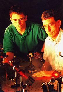
"We have a new technology for building the smallest mechanical devices," said Harold G. Craighead, Cornell professor of applied and engineering physics who has the directed the work performed by his doctoral student, Dustin W. Carr.
The guitar has six strings, each string about 50 nanometers wide, the width of about 100 atoms. If plucked — by an atomic force microscope, for example — the strings would resonate, but at inaudible frequencies. The entire structure is about 10 micrometers long, about the size of a single cell.
A scanning electron microscope photo of the guitar (see above) won the award for best scanning electron micrograph at the 41st Electron, Ion and Photon Beam Technology and Nanofabrication Conference in Dana Point, Calif., in May. Carr and Craighead presented their research at the conference and submitted a paper to the Journal of Vacuum Science and Technology.
While the guitar resulted in an award-winning electron micrograph, it is the other structures and devices that will be of real utility, Craighead says. Applications that require small-scale mechanical probes, high-speed response or measurement of very small forces can benefit from this technology. For example, mechanical force probes can be made much smaller than a single cell, and forces associated with single biological molecules could be measured.
An efficient and relatively non-invasive method of measuring the small motion of the mechanical structures is performed by using the interference of laser light beams. The Cornell researchers have made a Fabry-Perot interferometer using this technology. These interferometers use parallel mirrors, one of which moves relative to the other. The motion is detected by variations in the reflected light. The devices currently under study in Craighead's laboratories are moved by electrical forces. These electrically driven devices can be used to modulate the intensity of the reflected light.
"This could be of interest for light displays," said Craighead, former director of the Cornell Nanofabrication Facility, a national resource. "You could have arrays of these things because they're so small, with each one independently driveable. We have tremendous flexibility in what we can build."
In the near term, such nanostructures also can be used to modulate lasers for fiber optic communications. These researchers already have demonstrated the ability to make large amplitude modulation of light signals at high speeds. "We can make reflected light pulses at a rate of 12 million per second," Craighead said. Such a rate is faster than the bit rate of most ethernet connections.
The structures also are extremely sensitive to very small forces. "We make these structures move and measure the motion by placing single electrons on the surface of the devices," Carr said.
The key to the technology is electron-beam (or E-beam) lithography. E-beam lithography is a technique for creating extremely fine patterns (much smaller than can be seen by the naked eye) required by the modern electronics industry for integrated circuits. Derived from the early scanning-electron microscopes, the technique consists of scanning a beam of electrons across a surface covered with a thin film, called a resist. The electrons produce a chemical change in this resist, which allows the surface to be patterned.
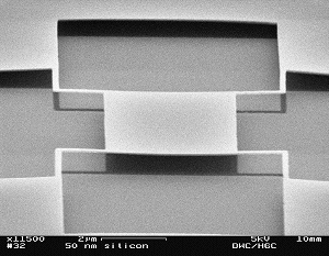
Most microelectromechanical devices are made by photolithography and chemical etching and have minimum feature sizes of slightly less than 1 micrometer. To build devices with dimensions of nanometers rather than micrometers requires a new fabrication approach.
A nanometer is one-billionth of a meter. For comparison, the diameter of a human hair is about 200 micrometers, or 200,000 nanometers — positively huge compared to these newest structures, where a wire is about 50 to 100 nanometers in diameter.
"I know we can go smaller than this. The question is how small we can go and still have dependable and measurable mechanical properties. That is one of the things we would like to know," Craighead said. "We are nearing the technological limit where it gets harder to get smaller than this."
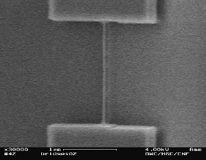
Using high-voltage electron beam lithography at the Cornell Nanofabrication Facility, one of only two similar machines in this country, Carr and Craighead sculpted their structures out of single crystal silicon on oxide substrates. A resist is used to pattern the top silicon layer. The oxide that is underneath this layer can be selectively removed using a wet chemical etch. The result: free-standing structures in silicon crystal.
"The nano-mechanical devices will also allow further exploration into important physical questions regarding motion and mechanical energy dissipation," the researchers wrote in their report.
The Cornell Nanofabrication Facility (CNF) at Cornell University, is partially supported by the National Science Foundation. It is part of the National Nanofabrication Users Network, a partnership of nanotechnology centers across the nation. In addition, this research was funded partially by the U.S. Department of Defense and the Department of Education.
Media Contact
Get Cornell news delivered right to your inbox.
Subscribe