Watching crystals grow provides clues to making smoother, defect-free thin films
By Anne Ju
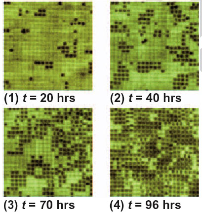
To make thin films for semiconductors in electronic devices, layers of atoms must be grown in neat, crystalline sheets. But while some materials grow smooth crystals, others tend to develop bumps and defects -- a serious problem for thin-film manufacturing.
In the Jan. 22 online edition of the journal Science, Cornell researchers shed new light on how atoms arrange themselves into thin films. Led by assistant professor of physics Itai Cohen, they recreated conditions of layer-by-layer crystalline growth using particles much bigger than atoms but still small enough that they behave like atoms.
"These particles are big and slow enough that you can see what's going on in real time," explained graduate student Mark Buckley.
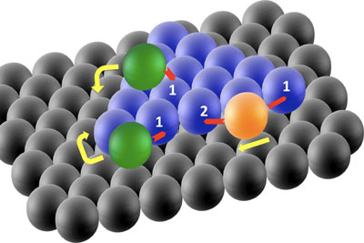
Using an optical microscope, the scientists could watch exactly what their "atoms" -- actually, micron-sized silica particles suspended in fluid -- did as they crystallized. What's more, they were able to manipulate particles one at a time and test conditions that led to smooth crystal growth. In doing so, they discovered that the random darting motion of the particles is a key factor that affects how the crystals grow.
A major challenge to growing thin films with atoms is that the atoms often form mounds, rather than crystallizing into thin sheets. This happens because as atoms are deposited onto a substrate, they initially form small crystals, called islands. When more atoms are dumped on top of these crystals, the atoms tend to stay atop the islands, rather than hopping off the edges -- as though there were a barrier on the crystals' edges. This creates the pesky rough spots, "and it's game over" for a perfect thin film, Cohen said.
Conventional theory says atoms that land on top of islands feel an energetic "pull" from other atoms that keeps them from rolling off. In their colloidal system, the researchers eliminated this pull by shortening the bonds between their particles. But they still saw their particles hesitate at the islands' edges.
Further analysis using optical tweezers to manipulate individual particles allowed the researchers to measure just how long it took for particles to move off the crystal islands. Because the particles were suspended in a fluid, they were knocked about in what's called Brownian motion, which is like a random walk.
As the particles moved and diffused from one area to another, the researchers noted that the distance a particle had to travel to "fall" off an island's edge was three times farther than moving laterally from one site on the island to another.
And because the particles had to go this distance in a Brownian fashion, it took them nine times longer to complete this "fall." This difference in time explained why the researchers still saw a barrier at their island edges.
Atoms on a crystalline film move in a manner similar to Brownian particles, since the vibrations of the underlying crystal, called phonons, tend to jostle them about. The researchers surmised that in addition to the bonding between the atoms, this random motion may also contribute to the barrier at the crystals' edges, and hence the roughness in the crystal film.
"If the principles we have uncovered can be applied to the atomic scale, scientists will be able to better control the growth of thin films used to manufacture electronic components for our computers and cell phones," Cohen said.
The paper's co-authors are former postdoctoral associate Rajesh Ganapathy, now a faculty member at the Jawaharlal Nehru Centre for Advanced Scientific Research in Bangalore, India, and graduate students Sharon Gerbode and Mark Buckley. The work was funded by King Abdullah University of Science and Technology, the Cornell Center for Materials Research, National Science Foundation and the Cornell NanoScale Science and Technology Facility.
Get Cornell news delivered right to your inbox.
Subscribe