In 'novel playground,' metals are formed into porous nanostructures for better fuel cells and microchips
By Bill Steele
For 5,000 years or so, the only way to shape metal has been to "heat and beat." Even in modern nanotechnology, working with metals involves carving with electron beams or etching with acid.
Now, Cornell researchers have developed a method to self-assemble metals into complex nanostructures. Applications include making more efficient and cheaper catalysts for fuel cells and industrial processes and creating microstructured surfaces to make new types of conductors that would carry more information across microchips than conventional wires do.
The method involves coating metal nanoparticles -- about 2 nanometers (nm) in diameter -- with an organic material known as a ligand that allows the particles to be dissolved in a liquid, then mixed with a block co-polymer (a material made up of two different chemicals whose molecules link together to solidify in a predictable pattern). When the polymer and ligand are removed, the metal particles fuse into a solid metal structure.
"The polymer community has tried to do this for 20 years," said Ulrich Wiesner, Cornell professor of materials science and engineering, who, with colleagues, reports on the new method in the June 27 issue of the journal Science. "But metals have a tendency to cluster into uncontrolled structures. The new thing we have added is the ligand, which creates high solubility in an organic solvent and allows the particles to flow even at high density."
Another key factor, he added, is to make the layer of ligand surrounding each particle relatively thin, so that the volume of metal in the final structure is large enough to hold its shape when the organic materials are removed.
"This is exciting," Wiesner said. "It opens a completely novel playground because no one has been able to structure metals in bulk ways. In principle, if you can do it with one metal you can do it with mixtures of metals."
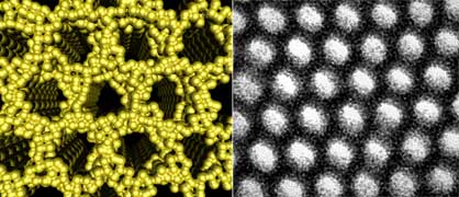
Wiesner and two Cornell colleagues, Francis DiSalvo, the J.A. Newman Professor of Chemistry and Chemical Biology, and Sol Gruner, the John L. Wetherill Professor of Physics, as well as other researchers, report in Science how they used the new method to create a platinum structure with uniform hexagonal pores on the order of 10 nm across (a nanometer is the width of three silicon atoms). Platinum is, so far, the best available catalyst for fuel cells, and a porous structure allows fuel to flow through and react over a larger surface area.
The researchers began by mixing a solution of ligand-coated platinum nanoparticles with a block co-polymer. The solution of nanoparticles combines with just one of the two polymers. The two polymers assemble into a structure that alternates between small regions of one and the other, in this case producing clusters of metal nanoparticles suspended in one polymer and arranged around the outside of hexagonal shapes of the other polymer. Many other patterns are possible, depending on the choice of polymers.
The material is then annealed in the absence of air, turning the polymers into a carbon scaffold that continues to support the shape into which the metal particles have been formed. Wiesner and colleagues have previously used the carbon scaffold approach to create porous nanostructures of metal oxides.
The final step is to heat the material to a higher temperature in air to oxidize the ligands and burn away the carbon. Metal nanoparticles have a very low melting point at their surface, so the particles sinter together into a solid metal structure. The researchers have made fairly large chunks of porous platinum this way, up to at least a half-centimeter across.
In addition to making porous materials, the researchers said, the technique could be used to create finely structured surfaces, the key to the new field of plasmonics, in which waves of electrons move across the surface of a conductor with the information-carrying capacity of fiber optics, but in spaces small enough to fit on a chip.
Get Cornell news delivered right to your inbox.
Subscribe